Use of logical border surfaces with reflectivity and transmittance

Hi All,

I have a geometry that goes something like this:

reflector->scintillator->glass->photocathode

I have defined these materials in the following, generic way:

In MyMaterial.cc:

void MyMaterial::DefineMaterials() {

...

//Material
  density=x*g/cm3;
  fmat = new G4Material(name="material",density,ncomponents=3,kStateSolid);
  fmat->AddElement(A,y*perCent);
  fmat->AddElement(B,z*perCent);
  fmat->AddElement(C,w*perCent);

//where x,y,z,w are numbers, and y+z+w = 100

}

void MyMaterial::DefineProperties() {

...

//---------------------------------------------------------------------------------
// Material
//---------------------------------------------------------------------------------

  G4MaterialPropertiesTable *myMat = new G4MaterialPropertiesTable();
  G4double  myMatRI[2], myMatAbs[2];
  myMatAbs[0] = a*mm;
  myMatAbs[1] = a*mm;
  myMatRI[0] = b ; 
  myMatRI[1] = b ; 
  G4double myMatEne[2] = {c*eV , d*eV} ;  
  
  myMat->AddProperty("RINDEX",   myMatEne , myMatRI,  2);
  myMat->AddProperty("ABSLENGTH", myMatEne, myMatAbs, 2);
  fMat->SetMaterialPropertiesTable(myMat);

...
}

In DetectorConstruction.cc:

...
G4VPhysicalVolume* GHDetectorConstruction::Construct()
{ 

...

//---------------------------------------------------------------------------------
// Reflector Material
//---------------------------------------------------------------------------------

 fSolidReflector  = new G4Tubs("SolidReflector", innerRadius, outerRadius, h, startAngle, spanningAngle) ;
 fLogicReflector  = new G4LogicalVolume(fSolidReflector, MyMaterial::Get()->GetMyMat() , "LogicReflector");
 fPhysicReflector = new G4PVPlacement(yRot,
                                 G4ThreeVector(x*cm, y*cm, z*cm), 
                                "ReflectorLayer",
                                fLogicReflector,
                                fPhysicWorld,
                                false,
                                0,
                                myCheckOverlap);
  fLogicReflector->SetVisAttributes( G4VisAttributes(myGreen) );;

...

 DefineSurfaces();


  return fPhysicWorld;
}

void DetectorConstruction::DefineSurfaces(){

G4double energy[2] = {e*eV, f*eV};
G4double ref[2] = {0.g, 0.g};
G4double tran[2] = {0.j, 0.j};

//---------------------------------------------------------------------------------
// Reflector-Air surface
//---------------------------------------------------------------------------------

G4OpticalSurface *fOpAirReflectorSurface = new G4OpticalSurface("OpAirReflectorSurface", glisur, ground, dielectric_metal, 0.1);
  new G4LogicalBorderSurface("AirReflectorSurface",fPhysicWorld , fPhysicReflector, fOpAirReflectorSurface); 

  G4MaterialPropertiesTable *fAirReflectorSurfProp = new G4MaterialPropertiesTable();
  fAirReflectorSurfProp->AddProperty("REFLECTIVITY", energy, ref, 2);
  fAirReflectorSurfProp->AddProperty("TRANSMITTANCE", energy, tran, 2);
  fOpAirReflectorSurface->SetMaterialPropertiesTable( fAirReflectorSurfProp );

  
  //---------------------------------------------------------------------------------
  // YAP-Reflector surface
  //---------------------------------------------------------------------------------

  G4OpticalSurface *fOpScintReflectorSurface = new G4OpticalSurface("OpScintReflectorSurface", glisur, polished, dielectric_metal, 1);
  new G4LogicalBorderSurface("ScintReflectorSurface", fPhysicScintCell, fPhysicReflector, fOpScintReflectorSurface); 

  G4MaterialPropertiesTable *fScintReflectorSurfProp = new G4MaterialPropertiesTable();
  fScintReflectorSurfProp->AddProperty("REFLECTIVITY", energy, ref, 2);
  fScintReflectorSurfProp->AddProperty("TRANSMITTANCE", energy, tran, 2);
  fOpScintReflectorSurface->SetMaterialPropertiesTable( fScintReflectorSurfProp );

...

}

I am using the physics list as suggested by the “OpNovice” example included during installation:

In my main function:

  G4VModularPhysicsList* physicsList = new FTFP_BERT;
  physicsList->ReplacePhysics(new G4EmLivermorePhysics());
  G4OpticalPhysics* opticalPhysics = new G4OpticalPhysics();
  physicsList->RegisterPhysics(opticalPhysics);
  runManager-> SetUserInitialization(physicsList);

With the rest of the material definitions defined in the ellipsis areas of the above script.
For clarity, I intend to shoot a gamma toward the reflector material, where it will next move into the scintillator, generate optical photons, which then propagate toward the photocathode.

My questions are:

  1. When defining the surfaces, and using a G4LogicalBorderSurface, is it necessary to define a surface going both ways? For example, in the case of the surface between the reflector and the scintillator, does one need to define the border with photons headed from the scintillator->reflector (dielectric_metal) and then another reflector->scintillator (not sure what this would be), or is it sufficient to only define one of these border surfaces?

  2. When defining the properties REFLECTIVITY and TRANSMITTANCE, does one need to define both, or is one sufficient, given that T = 100% - R (R = 100% - T)? I have read (Peculiarities in the Simulation of Optical Physics with Geant4) that when dealing with surfaces between dielectrics and metals, it is suggested to define the reflectivity, and when using dielectric to dielectric surfaces, that one should use the transmittance property.

  3. Also, if one were to use a dielectric as a reflector, example: a sheet of white paper, should the surface be defined as a dielectric_dielectric or a dielectric_metal?

Thank you all in advance for your help and guidance!

I am sorry if I previously posted this in the wrong section. Hopefully this is now posted under a more appropriate section.

-Frank
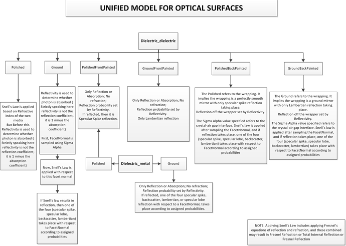
G4LogicalBorderSurfaces are defined separately for each direction of propagation. So yes, if your model requires a G4LogicalBorderSurface to accurately model reflector->scintillator transport, you will need to define it.

“A border surface is defined by specifying the ordered pair of physical volumes touching at the surface. Because the pair of physical volumes is ordered, the user may specify different optical properties for photons arriving from the reverse side of the same interface.” (Book for Application Developers)

This is incorrect. REFLECTIVITY is 1-(absorption coefficient). If you want a fraction f1 of photons absorbed, specify REFLECTIVITY = 1-f1. If you want a fraction f2 of photons transmitted, specify TRANSMITTANCE = f2. The rest undergo dielectric-dielectric interaction.

You’ll need to figure out what you want to simulate, and puzzle through the figure in the Book for Application Developers. Do you want opticalphotons propagating in the paper? Do you want total internal reflection? If either, dielectric_dielectric.

Thank you so much for replying to my post, @dsawkey I have a couple more questions if you don’t mind.

If I were to define a G4LogicalBorderSurface going from the reflector (metal) to the scintillator (dielectric) would I still use the dielectric_metal variable, and just change the order of the physical volumes, for example:

G4OpticalSurface *fOpReflectorScintSurface = new G4OpticalSurface("OpReflectorScintSurface", glisur, ground, dielectric_metal, 0.1);
new G4LogicalBorderSurface("ReflectorScintSurface", fPhysicReflector, fPhysicScintCell, fOpReflectorScintSurface);

Or is there another variable that I should use instead?

Thank you for clearing up my confusion with respect to how transmittance and reflectivity are defined. I think somehow I missed that flowchart in the the application developer’s handbook. Is it correct that f1 + f2 = 100% of the optical photons?

Thanks again for all of your help, time, and consideration regarding my questions.

-Frank

I’m not sure what you’re trying to do. If opticalphotons are generated in the scintillator, and the scintillator->reflector boundary is dielectric-metal, there shouldn’t be any opticalphotons in the reflector. Therefore there’s no need to specify a reflector->scintillator surface.

If you do want opticalphotons going both ways, then yes, define a fresh G4OpticalSurface and G4LogicalBorderSurface. The G4LogicalBorderSurface is created with arguments name, then preStep physical volume, then postStep physical volume.

No, the fraction (1-f1-f2) will undergo Fresnel refraction, Lambertian reflection, total internal reflection, etc.

Think of it starting from the ideal case of two dielectrics in perfect contact. Then REFLECTIVITY=1 (i.e. absorption = 0) and TRANSMITTANCE=0.

It’s very useful to play with the example extended/optical/OpNovice2, with macro boundary.mac. Edit it so there is one beamOn. The output will tell you what happens to the opticalphotons at the boundary.

You’re welcome!

Thanks again.

I am trying to simulate a gamma, shot into a column of materials. The gamma will first interact with the reflective layer, then a scintillator, glass and finally a photocathode.

reflector->scintillator->glass->photocathode

I assume that the gamma will transmit through the reflector, generate optical photons through scintillation, some of which will head toward the glass and photocathode and some towards the reflector. The optical photons will then ultimately be absorbed in the photocathode material.

From your comment, is it to be understood that since no optical photons will generate in the reflector volume, and merely be reflected/transmitted/absorbed by that volume, that it is only necessary to create a G4LogicalBorderSurface of which the scintillator would be the pre-step volume and the reflector would be the post-step volume? If I expect some of the optical photons to potentially be absorbed and transmitted, as well as be reflected by the reflector volume, what do you suggest I define?

Also, I know this is probably a very simple question, but does the G4OpticalSurfaceType with choices of dielectric_dielectric or dielectric_metal not refer to the order of the materials specified as the pre-step and post-step volume, as in if the pre-step is a metal and the post-step is a dielectric, we would still use the dielectric_metal option?

Ah yes, I really wasn’t thinking straight when I responded, thank you for clearing this up for me. Correct me again if I am wrong, but in the case of two dielectrics in perfect contact, isn’t there some instances when there will be some transmitted light from one material to the next?

Thank you again for all of your patience, time and consideration.

-Frank

If you’re going to want to have opticalphotons go from the reflector to the scintillator (e.g. if they are produced in the scintillator, go to the reflector, then back to the scintillator), then yes, you’ll want to think about that surface.

I’m not sure what you’re getting at. There’s no real concept in Geant4 of a material being a metal or dielectric. The terms dielectric_dielectric and dielectric_metal are simply for the surface. Inside the material, opticalphotons propagate based on the RINDEX and ABSORPTIONCOEFFICIENT etc. you specify. Are you thinking of evanescent waves or something?

The terminology is hard to work through. TRANSMITTANCE doesn’t refer to Fresnel refraction. Rather, if you want some fraction of the opticalphotons to pass through the boundary without interacting (so keeping the same momentum direction), specify a TRANSMITTANCE value.

For the scenario described then do two surfaces need to be defined or just one?

With regards to the difference between setting G4OpticalSurfaceType with either dielectric_dielectric or dielectric_metal, I was trying to see if the order of pre-step and post-step volumes had any relation to this variable, e.g. aluminum as pre-step and glass as post-step vs glass as pre-step and aluminum as post step. Your explanation here seems to clear this up, if not please let me know.

Thanks again for all of your help @dsawkey.

If the relevant surface isn’t defined, Geant4 will treat it as a perfect, flat, dielectric-dielectric surface.

See: Physics Processes — Book For Application Developers 11.2 documentation

Thank you again.

I am sorry for being so obtuse. I am not sure still on whether or not one needs to define two surfaces or one. My current understanding is that, if no surface is defined the surface will default to two perfectly flat dielectrics in contact. If a surface is defined, the program will take the settings of the surface as the variables for defining the post-step volume (i.e. its reflectivity, transmittance, etc.) beyond what is defined previously in its materials properties table.

I think my question is that in terms of the reflection, does one need to also define a surface for the volume in which the photons will reflect into, or is that taken care of by defining the surface from which the photons will be reflected?

Thank you again for your time and patience.

There’s a series of nested if statements that define this.
https://geant4.kek.jp/lxr/source/processes/optical/src/G4OpBoundaryProcess.cc#L295

Suppose the photon is moving from volume A to B. My understanding is:

  • if you use a G4LogicalBorderSurface: G4LogicalBorderSurface(A,B) is used if defined. G4LogicalBorderSurface(B,A) is ignored.
  • if you use a G4LogicalSkinSurface: one of G4LogicalSkinSurface(A) or G4LogicalSkinSurface(B) is used, depending on what is defined and if A is the mother volume of B.

Suppose A is not the mother of B. Use G4LogicalSkinSurface(A) if defined. Otherwise use G4LogicalSkinSurface(B) if defined. Otherwise, use the default of no surface (perfect dielectric-dielectric).

Unfortunately you’re going to have to do some investigation. I don’t know, definitively, what will happen for any given combination. My suggestion would be to put G4cout statements in G4OpBoundaryProcess at each of the if statements (linked above) and see what happens. Or run in a debugger.

@dsawkey Thank you so much for your time and consideration regarding my question. I will investigate this and if I come to any conclusions I will post them here.

@dsawkey for the simulation I am currently working on I set a G4LogicalBorderSurface for each potential direction of optical photon motion and saw no considerable difference for the number of photoelectrons generated by my photocathode and also the volumes in which optical photons are absorbed when having all surfaces defined versus just the ones that are expected (scintillation photons moving toward the reflector and potential transmission through the reflector into the world volume):

Example: G4LogicalBorderSurface of (prestep volume → poststep volume)

reflector->world volume, world volume->reflector, scintillator->reflector, reflector->scintillator

vs

reflector->world volume, scintillator->reflector ONLY

When defining only world volume->reflector and reflector->scintillator surfaces, I notice almost the reverse expected effect in terms of the number of photoelectrons generated and volumes in which optical photons are absorbed. I currently have the the reflector’s reflectivity set at 0.01 and transmittance at 0.99 uniformly for all energies. So when all surfaces for all directions are defined, I get a poor yield of photoelectrons and most of the optical photons are either absorbed into the reflector or transmitted out into the world volume, as I think is expected. Whereas when the surfaces that are less likely to see that direction of motion of optical photons are only defined the effect is to have more absorption/generation of optical photons in the photocathode and a minimum of transmission out into the world volume. I can provide my figures that represent this if you are interested.

Thanks again for all of your time, patience and consideration.

I’m not sure if you have a question. But this statement looks strange. Why call it a “reflector” if 99% if opticalphotons pass through the boundary as if it wasn’t there?

This topic was automatically closed 90 days after the last reply. New replies are no longer allowed.