Heavy Tail on High-Energy Side of Scintillation Photopeak

Geant4 Version: 4-11-04
Operating System: Ubuntu 22.04.5 LTS
Compiler/Version: g++ 11.4.0
CMake Version: 3.22.1


Greetings,

I am in the process of setting up a simulation for an array of LaBr3(Ce) scintillation detectors. To start, I have a single detector with simplified geometry: an Aluminium cylinder with the cylindrical scintillator crystal nested inside of it and a small optical photon tracking volume at the back to stand in for a SiPM. The GDML file below contains all the geometric details. The setup for the simulation is otherwise very similar to the OpNovice example provided with Geant4.

<?xml version="1.0" encoding="UTF-8" standalone="yes"?>
<gdml xmlns:xs="http://www.w3.org/2001/XMLSchema-instance" xs:noNamespaceSchemaLocation="http://cern.ch/service-spi/app/releases/GDML/schema/gdml.xsd">
	<define>
		<position name="pos_Tracker"  x="0.0" y="0.0" z="25.4" unit="mm"/>
		<position name="pos_Crystal"  x="0.0" y="0.0" z="-1.0" unit="mm"/>
		<position name="pos_Detector" x="0.0" y="0.0" z="79.2" unit="mm"/>
		<!--https://www.researchgate.net/publication/254060762_Optical_Absorption_Length_Scattering_Length_and_Refractive_Index_of_LaBr3Ce3-->
		<matrix coldim="2" name="LaBr3(Ce)_RINDEX"                     values="2.818*eV   2.18 3.875*eV  2.45"/>
		<matrix coldim="2" name="LaBr3(Ce)_RAYLEIGH"                   values="2.818*eV 159*mm 3.875*eV 88*mm"/>
		<matrix coldim="2" name="LaBr3(Ce)_ABSLENGTH"                  values="2.818*eV   10*m 3.468*eV  10*m 3.493*eV    240*mm 3.542*eV  52.54*mm 3.594*eV 14.57*mm 3.647*eV 5.852*mm 3.701*eV 2.739*mm 3.757*eV 1.492*mm 3.815*eV 0.5852*mm 3.875*eV  0.0*mm"/>
		<matrix coldim="2" name="LaBr3(Ce)_SCINTILLATIONCOMPONENT1"    values="2.817*eV    0.0 2.850*eV   0.0 2.883*eV 0.0001435 2.917*eV 0.0004305 2.952*eV 0.001148 2.988*eV 0.003157 3.024*eV 0.007750 3.061*eV  0.01464 3.100*eV   0.02511 3.139*eV 0.03774 3.179*eV 0.04937 3.220*eV 0.05626 3.241*eV 0.05755 3.263*eV 0.05755 3.306*eV 0.05697 3.328*eV 0.05841 3.351*eV 0.06228 3.397*eV 0.07893 3.444*eV 0.09544 3.468*eV 0.09931 3.493*eV 0.09673 3.542*eV 0.07577 3.594*eV 0.04262 3.647*eV 0.01737 3.701*eV 0.004592 3.757*eV 0.0007176 3.815*eV 0.0 3.875*eV 0.0"/>
		<matrix coldim="2" name="LaBr3(Ce)_SCINTILLATIONCOMPONENT2"    values="2.817*eV    0.0 2.850*eV   0.0 2.883*eV 0.0001435 2.917*eV 0.0004305 2.952*eV 0.001148 2.988*eV 0.003157 3.024*eV 0.007750 3.061*eV  0.01464 3.100*eV   0.02511 3.139*eV 0.03774 3.179*eV 0.04937 3.220*eV 0.05626 3.241*eV 0.05755 3.263*eV 0.05755 3.306*eV 0.05697 3.328*eV 0.05841 3.351*eV 0.06228 3.397*eV 0.07893 3.444*eV 0.09544 3.468*eV 0.09931 3.493*eV 0.09673 3.542*eV 0.07577 3.594*eV 0.04262 3.647*eV 0.01737 3.701*eV 0.004592 3.757*eV 0.0007176 3.815*eV 0.0 3.875*eV 0.0"/>
		<matrix coldim="1" name="LaBr3(Ce)_SCINTILLATIONTIMECONSTANT1" values="15.0*ns"/>
		<matrix coldim="1" name="LaBr3(Ce)_SCINTILLATIONTIMECONSTANT2" values="1.0*us"/>
		<matrix coldim="1" name="LaBr3(Ce)_SCINTILLATIONYIELD"         values="63.0/keV"/>
		<matrix coldim="1" name="LaBr3(Ce)_SCINTILLATIONYIELD1"        values="0.99"/>
		<matrix coldim="1" name="LaBr3(Ce)_SCINTILLATIONYIELD2"        values="0.01"/>
		<!--Resolution currently set to 0.5 of nominal value-->
		<matrix coldim="1" name="LaBr3(Ce)_RESOLUTIONSCALE"            values="0.5"/>
		<matrix coldim="2" name="LaBr3(Ce)_Al_REFLECTIVITY"            values="2.818*eV  0.9 3.875*eV  0.9"/>
		<matrix coldim="2" name="LaBr3(Ce)_Al_EFFICIENCY"              values="2.818*eV  1.0 3.875*eV  1.0"/>	
		<matrix coldim="2" name="LaBr3(Ce)_Tracker_REFLECTIVITY"       values="2.818*eV  1.0 3.875*eV  1.0"/>
		<matrix coldim="2" name="LaBr3(Ce)_Tracker_EFFICIENCY"         values="2.818*eV  1.0 3.875*eV  1.0"/>	
		<matrix coldim="2" name="Tracker_RINDEX"                       values="2.818*eV 2.18 3.875*eV 2.45"/>
		<matrix coldim="2" name="Tracker_ABSLENGTH"                    values="2.818*eV 1*um 3.875*eV 1*um"/>
	</define>
	<materials>
		<material formula=" " name="LaBr3(Ce)">
			<!--Density currently set to 1x actual value-->
			<D value="5.06" unit="g/cm3"/>
			<fraction n="0.3486" ref="G4_La"/>
			<fraction n="0.6331" ref="G4_Br"/>
			<fraction n="0.0183" ref="G4_Ce"/>
			<T unit="K" value="293"/>
			<property name="RINDEX"                     ref="LaBr3(Ce)_RINDEX"/>
			<property name="ABSLENGTH"                  ref="LaBr3(Ce)_ABSLENGTH"/>
			<property name="SCINTILLATIONCOMPONENT1"    ref="LaBr3(Ce)_SCINTILLATIONCOMPONENT1"/>
			<property name="SCINTILLATIONCOMPONENT2"    ref="LaBr3(Ce)_SCINTILLATIONCOMPONENT2"/>
			<property name="SCINTILLATIONTIMECONSTANT1" ref="LaBr3(Ce)_SCINTILLATIONTIMECONSTANT1"/>
			<property name="SCINTILLATIONTIMECONSTANT2" ref="LaBr3(Ce)_SCINTILLATIONTIMECONSTANT2"/>
			<property name="SCINTILLATIONYIELD"         ref="LaBr3(Ce)_SCINTILLATIONYIELD"/>
			<property name="SCINTILLATIONYIELD1"        ref="LaBr3(Ce)_SCINTILLATIONYIELD1"/>
			<property name="SCINTILLATIONYIELD2"        ref="LaBr3(Ce)_SCINTILLATIONYIELD2"/>
			<property name="RESOLUTIONSCALE"            ref="LaBr3(Ce)_RESOLUTIONSCALE"/>
		</material>
		<material formula="" name="Tracker">
			<D value="5.06" unit="g/cm3"/>
			<fraction n="0.3632" ref="G4_La"/>
			<fraction n="0.6331" ref="G4_Br"/>
			<fraction n="0.0037" ref="G4_Ce"/>
			<T unit="K" value="293"/>
			<property name="RINDEX" ref="Tracker_RINDEX"/>
			<property name="ABSLENGTH" ref="Tracker_ABSLENGTH"/>
		</material>
	</materials>
	<solids>
		<!-- Box geometry: -->
		<!-- x/y/z := the length of the side, i.e. -x/2 < p < x/2 -->
		<box name="geo_World" x="500" y="500" z="500" lunit="mm"/>
		<!-- Tube geometry: -->
		<!-- dx/dy := radius in x-y plane -->
		<!-- dz := half-length in the z direction, i.e. -dz < p < dz -->
		<eltube name="geo_Tracker" dx="19.05" dy="19.05" dz=" 1.0" lunit="mm"/>
		<eltube name="geo_Crystal" dx="19.05" dy="19.05" dz="25.4" lunit="mm"/>
		<eltube name="geo_Casing"  dx="21.05" dy="21.05" dz="27.4" lunit="mm"/>
		<!-- Optical surface defintion fot the LaBr3-Al casing interface -->
		<opticalsurface name="surface_LaBr3(Ce)_Al" finish="polished" model="glisur" type="dielectric_metal" value="1">
			<property name="REFLECTIVITY" ref="LaBr3(Ce)_Al_REFLECTIVITY"/>
			<property name="EFFICIENCY"   ref="LaBr3(Ce)_Al_EFFICIENCY"/>
		</opticalsurface>
		<opticalsurface name="surface_LaBr3(Ce)_Tracker" finish="polished" model="glisur" type="dielectric_dielectric" value="1">
			<property name="REFLECTIVITY" ref="LaBr3(Ce)_Tracker_REFLECTIVITY"/>
			<property name="EFFICIENCY"   ref="LaBr3(Ce)_Tracker_EFFICIENCY"/>
		</opticalsurface>
	</solids>
	<structure>
		<volume name="logvol_LaBr3(Ce)_Tracker">
			<materialref ref="Tracker"/>
			<solidref ref="geo_Tracker"/>
			<auxiliary auxtype="Sensitive_Detector" auxvalue="Tracker"/>
		</volume>
		<volume name="logvol_LaBr3(Ce)_Crystal">
			<materialref ref="LaBr3(Ce)"/>
			<solidref ref="geo_Crystal"/>
			<auxiliary auxtype="Sensitive_Detector" auxvalue="Crystal"/>
		</volume>
		<volume name="logvol_LaBr3(Ce)_Detector">
			<materialref ref="G4_Al"/>
			<solidref ref="geo_Casing"/>
			<physvol name="physvol_LaBr3(Ce)_Tracker">
				<volumeref ref="logvol_LaBr3(Ce)_Tracker"/>
				<positionref ref="pos_Tracker"/>
			</physvol>
			<physvol name="physvol_LaBr3(Ce)_Crystal">
				<volumeref ref="logvol_LaBr3(Ce)_Crystal"/>
				<positionref ref="pos_Crystal"/>
			</physvol>
		</volume>
		<volume name="World">
			<materialref ref="G4_AIR"/>
			<solidref ref="geo_World"/>
			<physvol name="physvol_LaBr3(Ce)_Detector">
				<volumeref ref="logvol_LaBr3(Ce)_Detector"/>
				<positionref ref="pos_Detector"/>
			</physvol>
		</volume>
		<bordersurface name="border_LaBr3(Ce)_Al" surfaceproperty="surface_LaBr3(Ce)_Al">
			<physvolref ref="physvol_LaBr3(Ce)_Crystal"/>
			<physvolref ref="physvol_LaBr3(Ce)_Detector"/>
		</bordersurface>
		<bordersurface name="border_LaBr3(Ce)_Tracker" surfaceproperty="surface_LaBr3(Ce)_Tracker">
			<physvolref ref="physvol_LaBr3(Ce)_Crystal"/>
			<physvolref ref="physvol_LaBr3(Ce)_Tracker"/>
		</bordersurface>
	</structure>
	<setup name="Default" version="0.0.2">
		<world ref="World"/>
	</setup>
</gdml>
 

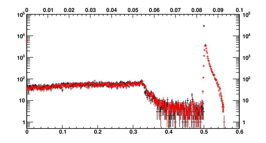
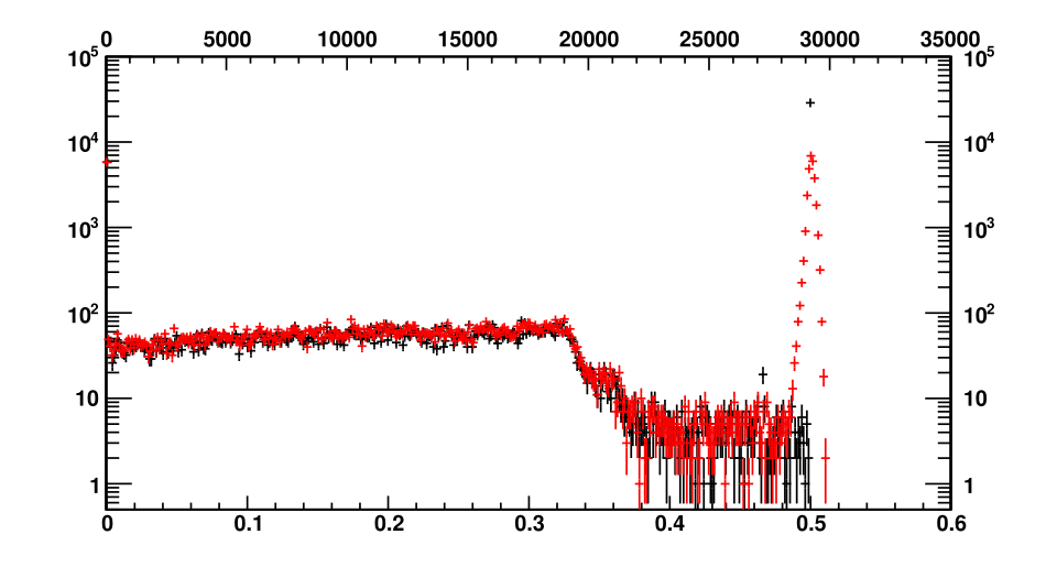
This seems to work reasonably well, except for a heavy high energy tail observed in the photopeak of the optical photon energy deposited in the tracking volume. For demonstration, I’ve run the simulation firing 500keV gammas into detector along it’s central axis. The histogram below tallies the energy deposited into the scintillation crystal by all processes excluding optical photons (black marks, using the bottom X axis) and the energy deposited in the tracking volume by only optical photons (red marks, using the top X axis).

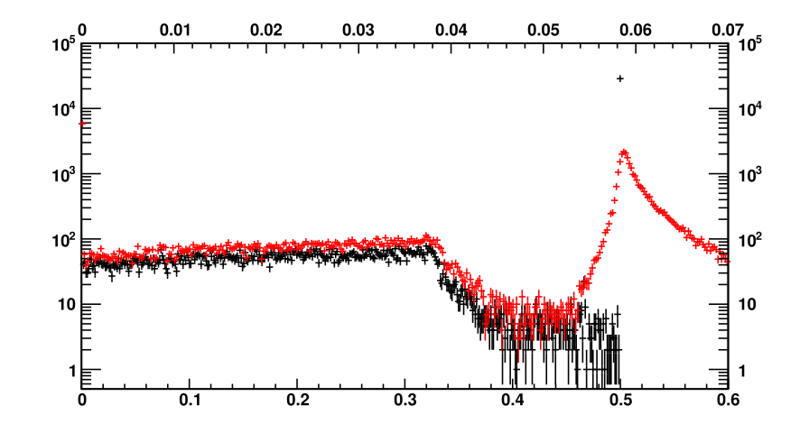
The simulation evidently works reasonably well for the prediction of the relative position of the photopeak and Compton edge, it really is just the shape of the photopeak that is not meeting expectations. My suspicion is that this is related to the fact that the the scintillation process doesn’t conserve energy, but I’m not 100% certain of that. Would anyone here know what might cause this? Of course, I might have made a mistake somewhere as well. I’m happy to share the code if requested, but the most likely source of problems there is (I think) the GDML file.

Thanks in advance!

If you don’t mind me asking, what is the reason you are tallying the optical photon energy deposition in your tracking volume? Please correct me if I am wrong, but that metric should be unrelated to the pulse height distribution you would expect to see out of your detector, i.e. that metric is should not be used to estimate the FWHM of your full energy peak.

I believe the reason you are seeing a correlation between the energy deposited by your primary gamma and the energy deposited by the optical photons is because you used the default Geant4 scintillation, which models light yield as a linear function of energy. The number of optical photons produced in your simulation then should posses a shape similar to the primary gamma ray energy deposition distribution, except broadened to account for your defined resolution scale.

My guess is that the reason your photon energy deposition distribution has a tail is because the photon transport probability throughout your device is not uniform. The further from your tracking volume interface you are, the more photons you are losing to absorption in the aluminum cylinder. It looks like you have it defined so that there is a 10% chance a photon is absorbed.

Hi Keith, thanks for the reply. My understanding is that pulse distribution one would observe from the SiPM is correlated to the number of photons impinging on it at any given moment, thus the integral of that should should more-or-less correlate to the total number of photons that strike the SiPM (or the energy they deposit, these are basically the same thing (excluding a scaling factor) due to the fairly narrow distribution of scintillation light). For the moment I’m after just this integral value.

I ran two other simulations to check whether or not the absorption is the cause of the heavy tail. One with a Aluminium-LaBr3 boundary reflectivity of 0.99 and one with 0.999. The 0.999 case is presented here:

The effect is fairly clear in comparison to the graph from my initial post. Increasing the reflectivity (decreasing the absorption) reduced the variance of the photopeak, but the heavy tail on the high-energy side remains. I will try increasing the absorption length of the optical photons in the LaBr3 crystal as well and post a reply only if there is a noticeable change.

David,

The answer given by jrellin to a question on a recent post does a good job of describing the phenomena which contribute to the variance of a full energy peak Simulated count variance much smaller than experimental — how to model realistic detector fluctuations? . I would say it is a worthwhile read for you. If you are trying to estimate a detector response for a detector you already have, then it would be much easier to simulate the energy deposition of a gamma ray in your system, (which you would statistically characterize) and then statistically broaden the energy deposition tally.

Back to the current question, I think the reason you are still observing a tail is because the optical photon emission spectrum you have defined. However, I would like to reiterate, a bit more strongly, that you should not use the energy deposited in your photomultiplier (PM) as a metric to estimate your full energy peak. While optical photon wavelength impacts the probability of reaching and interacting with and producing a photoelectron in a PM, it does not broaden the full energy peak the way that is shown in your graphs.

As a though experiment, let us assume that both a 3 and 6 eV photon have a 100% probability to reach the PM, likewise the PM sensitivity at these energies is also 100%. Furthermore we have magically altered our scintillator to only yield 3 and 6 eV photons. The question to ask then is, would energy deposition in the PM by photons be representative of our full energy peak. The answer would be no, this is true even if the variance introduced by the PM and readout electronics is negligible. This is because both a 3 and 6 eV photon would produce a single photoelectron in the PM. In short by using the energy deposition in the PM from optical photons as your metric, you are incorrectly introducing a broadening term.

If you set the scintillation parameters so that you only emit monoenergetic optical photons, then I think that high energy tail would go away.

Keith,

First, thank you for the link to that post. It’ll be a useful resource to me going forward.

The observed tail was indeed caused by the scintillation photon energy distribution as demonstrated in the graph below with the red data and top axis now represents only optical photon count absorbed in the tracker, not energy. Curiously, a test I had made counting the number of absorbed photons before changing the optical photon distribution to a Dirac delta still showed the heavy tail. My suspicion is that the absorption of the lower energy optical photons was the cause in that case.

Thanks for your assistance! Hopefully this thread of conversation is helpful to others in the future.

Just to reiterate, if you are trying to simulate a detector response function, you should tally the number of optical photons absorbed in your PM (NOT energy deposition).

As for why the metric you tallied had a high energy tail before defining your emission as mono-energetic, I think you are on the right track, but based on your absorption length vector it should actually be the high energy photons which are absorbed more frequently (not low energy). In fact based on your emission spectrum I had expected a low energy tail. What is likely occurring is that the high energy optical photons are being absorbed at a much higher frequency than the low energy.

For any future readers, I’d like to discuss Keith’s last point just a bit. He correctly points out that the higher energy photons are more likely to be absorbed than than the lower energy photons by a substantial amount. My current thinking on the matter is that we can break the optical photon emission spectra into essentially two parts. The first is a low energy component which will pass through the LaBr3 crystal (nearly) without absorption to the tracking volume where they can be tallied. This gives us the typical photopeak that we expect. The other portion is the high energy photons which are likely to be partially or entirely absorbed by the LaBr3 crystal before making it to the tracking volume unless they are generated quite close to it.

Together, this gives two components which are summed. The low energy portion is a gaussian due to the inherent variance of the scintillation photon production process in G4. The high energy portion is not simply described, but is a function of the absorption length, the distance from the tracker that high energy optical photons are spawned, and the probability of spawning high energy photons. This could be (very simplistically) approximated as an exponential decay.

Thus the baseline number of counts expected per event is provided by the low energy optical photons while there are sometimes more counts due to higher energy optical photons making it to the tracker. This explains why the tail is on the high energy side of the photopeak as opposed to Keith’s expectation of it being on the lower side.

However, this is all reliant on G4’s default scintillation process which may not behave in a necessarily physical way for the purposes of simulating detector responses to gamma energy deposition. Indeed, the documentation is not terribly clear on how the process actually works:

David,

The distribution that you are simulating is not representative of what you would see out of your detector; hence, I am not sure it is appropriate to call the Gaussian distribution you observe a photopeak since that term is usually applied to a pulse height distribution.

In a SiPM each pixel produces an avalanche of relatively the same magnitude per event, in other words the SiPM operates as a photon counter. That is why if you want to simulate a detector response function (including the photopeak) you need to count the number of photons which were absorbed in the SiPM (NOT the energy deposited in the SiPM). Sorry if I was a bit unclear about this.

I am not sure I agree with this. Fundamentally, there are four distributions that matter for the light transport.

  1. LaBr emission spectrum (what is generated)
  2. LaBr absorbtion spectrum (effectively optical trapping)
  3. SiPM window transmittance spectrum (needed for transmission to SIPM sensor)
  4. SiPM absorption spectrum (converting light into single photon pulses)

The difference between (1) and (2) are generally responsible for the Stoke’s Shift that you need for a useful scintillator. If they overlap completely none of that light can ever escape and its useless for a light sensor placed on the outside. 3 tends to be aggregated into 4 on vendor data sheets (Example: Figure 5) since they usually affix the window.

Geant4, and the optical/scintillation libraries let you define 1-4 above. None of these spectra are cleanly gaussian or exponential, and are also highly unique to the materials involved which is where R&D goes to optimize each of these. But @Keith-Huddleston is correct. SIPMs are silicon detectors operated in Geiger mode. What you really should be recording is photon counts to match to experimental data (you can of course still record the wavelength for optimization studies).

This topic was automatically closed 7 days after the last reply. New replies are no longer allowed.